- 您现在的位置:买卖IC网 > Sheet目录368 > W631GG6KB-15 (Winbond Electronics)IC DDR3 SDRAM 1GBIT 96WBGA
�� �
�
�W631GG6KB�
�10.7� DC� and� AC� Output� Measurement� Levels�
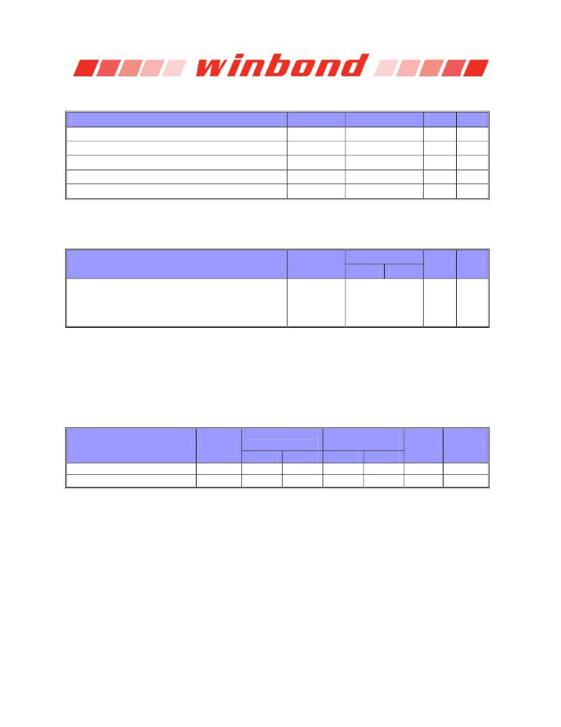
�Table� 24� –� Single-ended� DC� and� AC� Output� Levels�
�PARAMETER�
�DC output high measurement level (for IV curve linearity)�
�DC� output� mid� measurement� level� (for� IV� curve� linearity)�
�DC� output� low� measurement� level� (for� IV� curve� linearity)�
�AC� output� high� measurement� level� (for� output� slew� rate)�
�AC� output� low� measurement� level� (for� output� slew� rate)�
�SYMBOL�
�V� OH(DC)�
�V� OM(DC)�
�V� OL(DC)�
�V� OH(AC)�
�V� OL(AC)�
�VALUE�
�0.8� x� V� DDQ�
�0.5� x� V� DDQ�
�0.2� x� V� DDQ�
�V� TT� +� 0.1� x� V� DDQ�
�V� TT� -� 0.1� x� V� DDQ�
�UNIT�
�V�
�V�
�V�
�V�
�V�
�NOTES�
�1�
�1�
�Note:�
�1.� The� swing� of� ±� 0.1� ×� V� DDQ� is� based� on� approximately� 50%� of� the� static� single-ended� output� high� or� low� swing� with� a�
�driver� impedance� of� 34� Ω� and� an� effective� test� load� of� 25� Ω� to� V� TT� =� V� DDQ� /2.�
�Table� 25� –� Differential� DC� and� AC� Output� Levels�
�PARAMETER�
�AC� differential� output� high� measurement� level� (for� output�
�slew� rate)�
�AC� differential� output� low� measurement� level� (for� output�
�slew� rate)�
�SYMBOL�
�V� OH.DIFF(AC)�
�V� OL.DIFF(AC)�
�VALUE�
�MIN.� MAX.�
�+0.2� x� V� DDQ�
�-0.2� x� V� DDQ�
�UNIT�
�V�
�V�
�NOTES�
�1�
�1�
�Note:�
�1.� The� swing� of� ±� 0.2� ×� V� DDQ� is� based� on� approximately� 50%� of� the� static� single-ended� output� high� or� low� swing� with� a�
�driver� impedance� of� 34� Ω� and� an� effective� test� load� of� 25� Ω� to� V� TT� =� V� DDQ� /2� at� each� of� the� differential� outputs.�
�10.7.1� Output� Slew� Rate� Definition� and� Requirements�
�The� slew� rate� definition� depends� if� the� signal� is� single-ended� or� differential.� For� the� relevant� AC� output�
�reference� levels� see� above� Table� 24� and� Table� 25.�
�Table� 26� –� Output� Slew� Rate�
�PARAMETER�
�SYMBOL�
�DDR3-1333,�
�DDR3-1600�
�MIN.�
�MAX.�
�DDR3-1866�
�MIN.�
�MAX.�
�UNIT�
�NOTES�
�Single-ended� Output� Slew� Rate�
�Differential� Output� Slew� Rate�
�SRQse�
�SRQdiff�
�2.5�
�5�
�5�
�10�
�2.5�
�5�
�5*� 1�
�12�
�V/nS�
�V/nS�
�1,� 2,� 3�
�2,� 3�
�Notes:�
�1.� In� two� cases,� a� maximum� slew� rate� of� 6� V/nS� applies� for� a� single� DQ� signal� within� a� byte� lane.�
�-� Case� 1� is� defined� for� a� single� DQ� signal� within� a� byte� lane� which� is� switching� into� a� certain� direction� (either� from� high�
�to� low� or� low� to� high)� while� all� remaining� DQ� signals� in� the� same� byte� lane� are� static� (i.e� they� stay� at� either� high� or� low).�
�-� Case� 2� is� defined� for� a� single� DQ� signal� within� a� byte� lane� which� is� switching� into� a� certain� direction� (either� from� high�
�to� low� or� low� to� high)� while� all� remaining� DQ� signals� in� the� same� byte� lane� are� switching� into� the� opposite� direction� (i.e.�
�from� low� to� high� or� high� to� low� respectively).� For� the� remaining� DQ� signal� switching� into� the� opposite� direction,� the�
�regular� maximum� limit� of� 5� V/nS� applies.�
�2.� Background� for� Symbol� Nomenclature:� SR:� Slew� Rate;� Q:� Query� Output� (like� in� DQ,� which� stands� for� Data-in,� Query-�
�Output);� se:� Single-ended� Signals;� diff:� Differential� Signals.�
�3.� For� R� ON� =� RZQ/7� settings� only.�
�Publication� Release� Date:� Dec.� 09,� 2013�
�Revision� A05�
�-� 107� -�
�发布紧急采购,3分钟左右您将得到回复。
相关PDF资料
W9412G6IH-5
IC DDR-400 SDRAM 128MB 66TSSOPII
W9412G6JH-5I
IC DDR SDRAM 128MBIT 66TSOPII
W9425G6EH-5
IC DDR-400 SDRAM 256MB 66TSSOPII
W9425G6JH-5I
IC DDR SDRAM 256MBIT 66TSOPII
W947D2HBJX5E
IC LPDDR SDRAM 128MBIT 90VFBGA
W948D2FBJX5E
IC LPDDR SDRAM 256MBIT 90VFBGA
W949D2CBJX5E
IC LPDDR SDRAM 512MBIT 90VFBGA
W971GG6JB25I
IC DDR2 SDRAM 1GBIT 84WBGA
相关代理商/技术参数
W631GG8KB-11
制造商:Winbond Electronics Corp 功能描述:IC DDR3 SDRAM 1GBIT 制造商:Winbond Electronics Corp 功能描述:IC DDR3 SDRAM 1GBIT 78WBGA
W631GG8KB-12
制造商:Winbond Electronics Corp 功能描述:DRAM Chip DDR3 SDRAM 1G-Bit 128Mx8 1.5V 制造商:Winbond Electronics Corp 功能描述:IC DDR3 SDRAM 1GBIT 制造商:Winbond Electronics Corp 功能描述:IC DDR3 SDRAM 1GBIT 78WBGA
W631GG8KB-15
制造商:Winbond Electronics Corp 功能描述:IC DDR3 SDRAM 1GBIT 制造商:Winbond Electronics Corp 功能描述:IC DDR3 SDRAM 1GBIT 78WBGA
W632
制造商:LUMINIS 制造商全称:LUMINIS 功能描述:Wall mount
W632GG6KB-11
制造商:Winbond Electronics Corp 功能描述:IC DDR3 SDRAM 2GBIT 96WBGA
W632GG8KB-11
制造商:Winbond Electronics Corp 功能描述:IC DDR3 SDRAM 2GBIT 78WBGA
W634
制造商:LUMINIS 制造商全称:LUMINIS 功能描述:Wall mount
W638
制造商:LUMINIS 制造商全称:LUMINIS 功能描述:Wall mount